HKUST Research Team Expands the Horizon and Explores New Frontiers of Wide-bandgap GaN Integration by Introducing Two New Technologies in IEDM 2021
A research team led by Prof. Kevin Chen of Department of Electronic and Computer Engineering at The Hong Kong University of Science and Technology (HKUST), has recently introduced two new technologies for wide-bandgap semiconductor gallium nitride (GaN) integration in 2021 IEDM (International Electron Device Meeting), San Francisco, USA, 11-15 December 2021. IEDM is the most prominent forum for reporting technological breakthroughs in the areas of semiconductor and related device technologies, design, manufacturing, physics, modeling and circuit-device interaction.
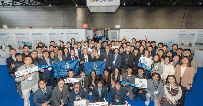
In back-to-back presentations in the session of “Power Devices and Systems – GaN Power Devices, Technologies, and Circuits”, HKUST team reported (1) “A GaN Power Integration Platform based on Engineered Bulk Si Substrate with Eliminated Crosstalk between High-Side and Low-Side HEMTs” (by Gang Lyu, et al.) and (2) “SiN/in-situ-GaON Staggered Gate Stack on p-GaN for Enhanced Stability in Buried-Channel GaN p-FETs” (by Li Zhang, et al.). Year 2021 also marked the 30th presentation in IEDM by Prof. Chen’s team as well as the 30th Anniversary of HKUST.
Half-bridge converters, featuring high-side and low-side power switches, are essential to many mainstream power converters to deliver high output power at compact size and competitive cost. Monolithic integration of high- and low-side power switches could play an important role in unlocking the full potential of GaN power electronics in high-frequency switching, but has been hindered by the inherent crosstalk through the Si substrate (used to grow GaN epi-structures for power devices) for years. By expanding the role of silicon substrate beyond a platform for epitaxial growth, embedded P-N junctions are designed and implemented in Si substrate to provide effective isolation with nearly ideal elimination of crosstalk between high- and low-side GaN switches, without the need to change GaN growth conditions or use the more expensive SOI (silicon-on-insulator) substrates.
GaN complementary logic (or CMOS) integrated circuits, which could provide GaN-based electronics systems with enhanced intelligence and control have witnessed key breakthroughs recently. The gate stack for GaN p-FETs is one of the first crucial issues for a practically viable GaN CMOS technology. With an unconventionally designed SiN/GaON structure, a gate dielectric with staggered valence-band energy profiles, interface traps are substantially removed. Hysteresis-free GaN p-FETs and GaN CMOS ring oscillators with stable frequency are reported for the first time.


